

How a Processor is Made?
- Sukesh Kumar Reddy

- Apr 4, 2020
- 4 min read
Step 1 – Sand
At about 25% (by mass), silicon is the second most frequent chemical in the earth’s crust (behind oxygen). Sand has a high percentage of Silicon Dioxide (SiO2), which is the base ingredient for semiconductor manufacturing.
Step 2 – Melted Silicon
Silicon is purified in multiple steps to reach the Electronic Grade Silicon used in semiconductors. It ultimately arrives in mono crystal ingots about 12″ in diameter (300mm today, the older ingots were 8″ or 200mm in diameter and smaller — the first wafers in the 1970s were 2″ in diameter, or 50mm).
The purity at this level of refinement is about one part per billion, meaning only one foreign atom per billion silicon atoms. The ingot weighs about 220lbs, and is a 99.9999% pure vertical column of slick glass-looking material.
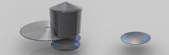
Step 3 – Ingot Slicing
The ingot is cut with a very thin saw into individual silicon slices (called wafers), each of which are then polished to a flawless mirror-smooth surface. It is upon this totally smooth wafer surface that the tiny copper wires are deposited in the following several steps.

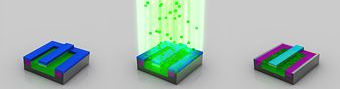
Step 4 – Photo Resist, Exposure
A photo resist liquid is poured onto the wafer while it spins at high speed (similar to materials used in conventional photography). This spinning deposits a thin and even resist layer across the entire surface.
From there, an ultraviolet laser is shone through masks and a lens (which make a focused image 4x smaller than the mask) causing tiny illuminated UV lines on the surface. Everywhere these lines strike the resist, a chemical reaction takes place making those portions soluble.
Step 5 – Washing, etching
The soluble photo resist material is then completely dissolved by a chemical solvent. From there, an etching chemical is used to partially dissolve (or etch) away a tiny quantity of the polished semiconductor material (the substrate). Finally, the remainder of the photo resist material is removed through a similar washing process, revealing the etched surface of the wafer.
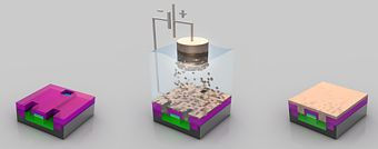
Step 6 – Building up layers
In order to create the tiny copper wires which ultimately convey electricity to/from the chip’s various connectors, additional photo resists are added, exposed and washed. Next, a process called ion implantation is used to dope and protect locations where copper ions are deposited from a copper sulfate solution in a process called electroplating.
At various stages during these processes, additional materials are added, exposed, washed / etched and polished. This process is repeated six times for six-layer processes, which is reportedly what Intel uses for their current 45nm high-k, metal gate processes.
The final product looks like a jungle gym, a a host of tiny copper bars which convey electricity. Some of these are connected, some are exactly a specific distance away from other ones. And all of them are used for one purpose: To convey electrons, wielding their electromagnetic effects in a particular way to conduct what we would call “useful work” (such as adding two numbers together at extremely high rates of speed, the very essence of modern day computing).
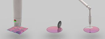
Step 7 – Testing
Once all of the metal layers are built up, and the circuits (transistors) are all created, it’s time for testing. A device with lots of prongs sits down on top of the chip, attaching microscopic leads to the chip’s surface. Each lead completes an electrical connection within the chip, simulating how it would operate in final form once packaged into end-consumer products.
A series of test signals are sent to the chip with whatever the results are being read. This level of testing includes not only traditional computational abilities, but also internal diagnostics along with voltage readings, cascade sequences (does data flow through as it should), etc. And however the chip responds as a result of this testing, is what’s stored in a database assigned specifically for that die.
This process is repeated for every die on the entire wafer’s surface while all dies are still on the surface.
Step 8 – Slicing
A tiny diamond-tipped saw is used to cut the silicon wafer into its various dies. The database derived in Step 7 is used to determine which chips cut from the wafer are kept, and which are discarded. The ones which produced “the right results” in Step 7’s testing are kept, with the rest being thrown away.
Step 9 – Packaging
At this point, all working dies get put into a physical package. It’s important to note that while they’ve had preliminary tested and were found to operate correctly, this doesn’t mean they’re good CPUs.
The physical packaging process involves placing the silicon die onto a green substrate material, to which tiny gold leads are connected to the chip’s pins or ball grid array, which show through the bottom side of the package. On the top of that, a heat spreader is introduced. This appears as the metal package on top of a chip. When finished, the CPU looks like a traditional package end-consumers buy.
Note: The metal heat spreader is a crucial component on modern high-speed semiconductors. In the past, a ceramic top was used with no active cooling. It wasn’t until the 80386 and later time frame, along with some extreme high-speed 8086 and 80286 (100MHz models), that active cooling was required. Prior to that, the chips had so few transistors (the original 8086 had 29K, today’s CPUs have 100s of millions) that they didn’t generate enough heat to require active cooling. To separate themselves, these later ceramic chips were stamped with the warning: “Heatsink required”.
Modern CPUs generate enough heat to melt themselves in a few seconds. Only by having the heat spreader connected to a large heat sink (and fan) can they operate long-term as they do.
Step 10 – Binning
At this point the package looks like you or I will buy it. Still, there is one more step involved. This final step is called binning.
In this process, the actual characteristics of this particular CPU is measured. Items such as voltage, frequency, performance, heat generation and other internal operational characteristics of its cache, for example, are all measured.
The best chips are generally binned as higher-end parts, being sold as not only the fastest parts with their full caches enabled, but also the low-voltage and ultra low-voltage models. Note: Based on market demand, these highest-end chips can also be sold as lesser chip parts.
Chips which do not perform as well as the best chips are often sold for lower clock speed models, or as a triple- or dual-core (Phenom X3, Phenom X2) instead of their native quad-core. Others may have half their cache disabled (Celeron), etc.


Comments